- 您现在的位置:买卖IC网 > Sheet目录1994 > DS26503LN+ (Maxim Integrated Products)IC T1/E1/J1 BITS ELEMENT 64-LQFP
DS26503 T1/E1/J1 BITS Element
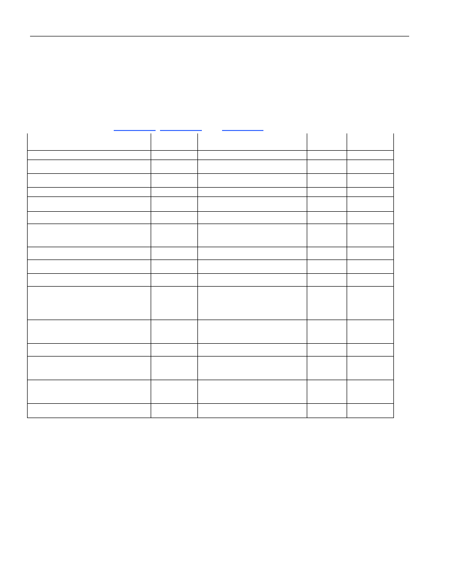
(VDD = 3.3V ±5%, TA = 0°C to +70°C for DS26503L; VDD = 3.3V ±5%, TA = -40°C to +85°C for
DS26503LN.) (Note 1, Figure 19-1
19. AC TIMING PARAMETERS AND DIAGRAMS
Capacitive test loads are 40pF for bus signals and 20pF for all others.
19.1 Multiplexed Bus
Table 19-1. AC Characteristics, Multiplexed Parallel Port
NOTES
PARAMETER
SYMBOL
MIN
TYP
MAX
UNITS
Cycle Time
tCYC
200
ns
Pulse Width,
DS Low or RD High
PWEL
100
ns
Pulse Width,
DS High or RD Low
PWEH
100
ns
Input Rise/Fall Times
tR, tF
20
ns
R/
W Hold Time
tRWH
10
ns
R/
W Setup Time Before DS High
tRWS
50
ns
CS Setup Time Before DS, WR, or
RD Active
tCS
20
ns
tCH
0
ns
Read-Data Hold Time
tDHR
10
50
ns
Write-Data Hold Time
tDHW
5
ns
Muxed Address Valid to AS or
ALE Fall
tASL
15
ns
Muxed Address Hold Time
tAHL
10
ns
Delay Time
DS, WR, or RD to AS
or ALE Rise
tASD
20
ns
Pulse Width AS or ALE High
PWASH
30
ns
Delay Time, AS or ALE to
DS,
WR, or RD
tASED
10
ns
Output Data Delay Time from
DS
or
RD
tDDR
80
ns
Data Setup Time
tDSW
50
ns
CS Hold Time
Note 1:
The timing parameters listed in this table are guaranteed by design (GBD).
110 of 122
发布紧急采购,3分钟左右您将得到回复。
相关PDF资料
DS3105LN+
IC TIMING LINE CARD 64-LQFP
DS3106LN+
IC TIMING LINE CARD 64-LQFP
DS3231MZ+
IC RTC I2C 8SOIC
DS3231SN#T&R
IC RTC W/TCXO 16-SOIC
DS3232MZ+
IC RTC W/SRAM I2C 8SOIC
DS3232SN#T&R
IC RTC W/TCXO 20-SOIC
DS3234S#
IC RTC W/TCXO 20-SOIC
DS32C35-33#T&R
IC RTC ACCURATE I2C 3.3V 20-SOIC
相关代理商/技术参数
DS26504
制造商:Maxim Integrated Products 功能描述:T1/E1/J1 ENH BITS ELEMENT LQFP - Trays
DS26504_06
制造商:MAXIM 制造商全称:Maxim Integrated Products 功能描述:T1/E1/J1/64KCC BITS Element
DS26504DK
功能描述:网络开发工具 DS26504 Dev Kit RoHS:否 制造商:Rabbit Semiconductor 产品:Development Kits 类型:Ethernet to Wi-Fi Bridges 工具用于评估:RCM6600W 数据速率:20 Mbps, 40 Mbps 接口类型:802.11 b/g, Ethernet 工作电源电压:3.3 V
DS26504L
功能描述:计时器和支持产品 E1/T1/J1/64Kcc Bits Element RoHS:否 制造商:Micrel 类型:Standard 封装 / 箱体:SOT-23 内部定时器数量:1 电源电压-最大:18 V 电源电压-最小:2.7 V 最大功率耗散: 最大工作温度:+ 85 C 最小工作温度:- 40 C 封装:Reel
DS26504L+
功能描述:计时器和支持产品 E1/T1/J1/64Kcc Bits Element RoHS:否 制造商:Micrel 类型:Standard 封装 / 箱体:SOT-23 内部定时器数量:1 电源电压-最大:18 V 电源电压-最小:2.7 V 最大功率耗散: 最大工作温度:+ 85 C 最小工作温度:- 40 C 封装:Reel
DS26504LN
功能描述:计时器和支持产品 E1/T1/J1/64Kcc Bits Element RoHS:否 制造商:Micrel 类型:Standard 封装 / 箱体:SOT-23 内部定时器数量:1 电源电压-最大:18 V 电源电压-最小:2.7 V 最大功率耗散: 最大工作温度:+ 85 C 最小工作温度:- 40 C 封装:Reel
DS26504LN+
功能描述:计时器和支持产品 E1/T1/J1/64Kcc Bits Element RoHS:否 制造商:Micrel 类型:Standard 封装 / 箱体:SOT-23 内部定时器数量:1 电源电压-最大:18 V 电源电压-最小:2.7 V 最大功率耗散: 最大工作温度:+ 85 C 最小工作温度:- 40 C 封装:Reel
DS26504LN+T&R
制造商:Maxim Integrated Products 功能描述:T1/E1/J1 ENH BITS IC LQFP LF T&R - Tape and Reel 制造商:Maxim Integrated Products 功能描述:IC T1/E1/J1 64KCC ELEMENT 64LQFP